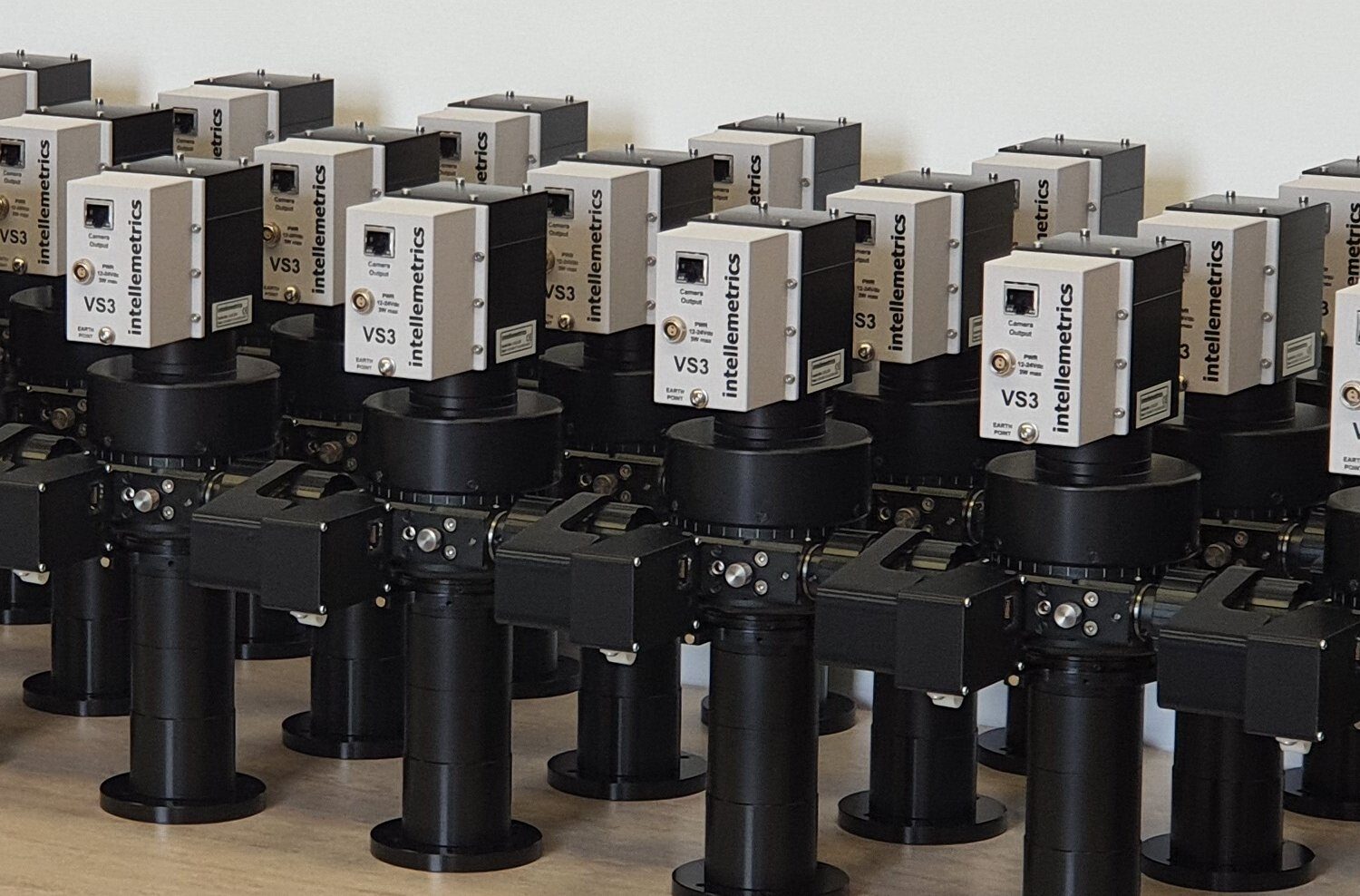
Intellemetrics introduces a range of Wafer Vision Systems specially design for viewing patterned semiconductor wafers within load-locked vacuum and deposition chambers in order to check that the correct wafter has been loaded, and to confirm alignment and placement with respect to the mask pattern.
Image resolution depends upon the working distance and field of view, but typically resolutions of 5µm can be obtained at working distances of 600mm (ideal for ICP chambers) and fields of view of 7mm.
Features include:
A batch of wafer imaging systems fully tested prior to shipping to a premier etch system OEM.