Over 200 layers were modelled using EtchDirector’s modelling capability as shown in the left-hand window.
The right-hand window shows the results from the actual etch run. The LEP500 reproduced the modelled data to a high degree and detected each turning point during the run enabling the progress of the etch to be followed and for the process to endpoint with a high degree of accuracy.
The LEP500’s combination of modelling and monitoring capability removed the need for 4-5 ‘vent-&-measure’ steps or performance of numerous sacrificial calibration runs, saving significant time and expensive epi-wafers.
The level of certainty achievable with the LEP500 becomes even more critical for devices requiring multiple etch stages.
The achievable etch stop accuracy in this case was around 5nm.

As the graph above indicates, the LEP500 can be used to monitor the etch back of dielectric on metal for a number of applications including failure analysis.
The LEP500 monitors a small (approx 20 micron diameter) exposed area and is therefore ideal for monitoring one small chip in an entire chamber – unlike optical emission spectroscopy which would struggle to detect such dilute species.
EtchDirector utilises an advanced end point algorithm to detect the ‘flat-line’ at the end of the oxide etch. In field tests, EtchDirector reliably detects the endpoint well before a skilled operator, thereby avoiding unwanted removal, damage or contamination of the underlying Al layer. The endpoint algorithm also allows the user to enter an overetch time to enable full clearout across the wafer.
A major advantage of this algorithm is that reliable endpointing does not depend upon the starting oxide thickness. This is especially important in a manufacturing environment where pre-measurement of the oxide thickness is prohibitive in terms of time and cost.
The LEP500 is also ideal for monitoring the etch of SiN on metal or even combinations of SiN on SiO2 or on Si.

Metals are not transparent until very thin and therefore you cannot obtain interference fringes and monitor etch depth & rate through the bulk of a metal layer.
However, the LEP500 is ideal for picking out interfaces, indicated by a step level change in reflectivity. The above example shows titanium being etched from a LiNbO3 substrate. Whilst monitoring at 670nm, the large drop in signal occurs over an etch depth of less than 30nm. EtchDirector comes with an endpoint algorithm specifically designed to identify this step level change and enables the operator to choose whether to stop at the top, middle or bottom of the curve. Again, an overetch capability is also included to enable a clearout etch to be achieved.
A major advantage of this algorithm is that reliable endpointing does not depend upon the starting metal thickness. This is especially important in a manufacturing environment where premeasurement of the metal thickness is prohibitive in terms of time and cost.
This process works even at high etch rates and has been proven to be faster and more accurate than a skilled operator. The process works equally well for other metals including NiCr, Ni, Au, Tg, Pt, etc, and works for a wide range of substrates.

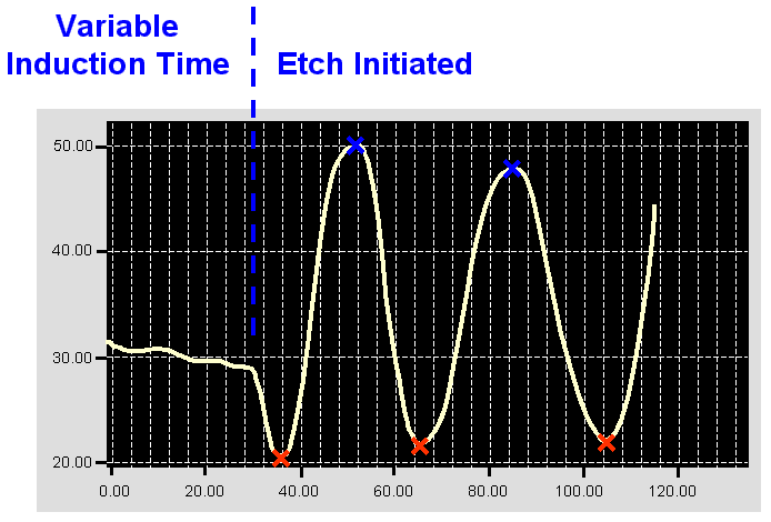
Selective low damage plasma etch processes are used in a number of applications including III-V etching of InP & GaAs HEMTs and for active III-V optoelectronic devices including lasers, modulators and detectors. Often these processes experience an induction period at the beginning of the etch process during which the native oxide, and/or residues from the previous process stage, inhibit the etch. Once this layer has been removed the etch proceeds as normal.
The problem is that the induction time is variable and may become a significant proportion of the expected etch duration. Without in-situ monitoring this can lead to large uncertainties in the etch depth.
The LEP500 enables the operator to actually ‘see’ the induction period, as shown in the graph above, and still obtain a highly accurate and repeatable etch process.

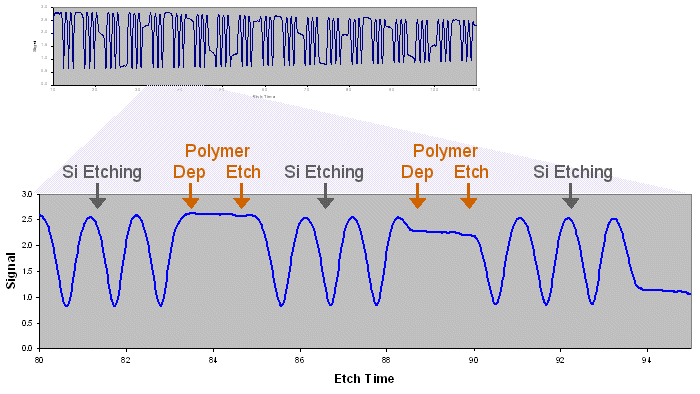
The ‘Bosch’ ICP etch process is widely used to achieve extremely high etch rate (> 20 microns per minute) high aspect ratio (> 100:1) etching of silicon microstructures used throughout the MEMS industry. It is a switched process characterised by alternate stages of silicon etch, polymer deposition, polymer etchback, and silicon etch again. This process is cycled until the required etch depth is achieved.
Although the process is extremely successful, it does have some issues. The first of these is that the etch rate is significantly dependant upon the lateral feature sizes as well as the mask-to-open-area ratio. The second of these is the fact that the polymer etchback time is variable as it depends upon the precise etch/dep parameters as well as the mask geometry and is therefore essentially outwith the control of the operator. This is compounded by the fact that the precise etch parameters are often ‘tweaked’ to achieve the verticality and smoothness for a particular mask design.
This means that every time a new mask design is used, or if the etch parameters are tweaked, then time consuming full-wafer dummy etches need to be undertaken to measure the etch depth and therefore calibrate the etch rate.
Use of the LEP500 completely avoids these stages and even avoids the need to measure the etch depth post etch using a profilometer.
EtchDirector incorporates high speed shape recognition algorithms that analyse the shape of the reflected signal thereby tracking the silicon etch and rejecting the polymer deposition and etchback stages. The LEP500 can precisely follow etch rates in excess of 20 microns per minute.